Division of Physics of Dielectrics and Semiconductors

Laboratory of Kinetic Phenomena in Solids at Low Temperatures

Physics of tellurium

Leading by

Iosif Farbshtein, Principal Researcher

Vyaecheslav Berezovets, Senior Researcher

Robert Parfen'ev, Professor

 Sergey Yakimov, Junior Researcher

 
Goal: the study of the elementary semiconductor with a unique anisotropic structure.
Objects: high quality single crystal Te and low-dimensional tellurium – based structures
Methods: dc electric measurements of classical and quantum effects, measurements of optical activity, high pressure studies at 0.4 K< T<300 K, H<12 T (dc) and H<35 T (pulse), p<14 kbar.

• High quality Te single crystals (extremely pure and doped by Sb) have been obtained by Czohralsky method. The peculiarities of crystal growth at different gravity levels have been determined.
 • Galvanomagnetic properties in low magnetic field and their dependence on the amount of structural defects have been investigated.
• The shape of the hole Fermi surface in Tellurium and its evolution with concentration of careers have been determined. The dispersion law of the Te valence band have been calculated.
• The transformation of Te valence band by hydrostatic pressure have been measured.
• The optical activity of tellurium near the band edge and optical translucence have been measured and compared with the developed theory.
• The 2D layer on the different Te crystal surfaces have been created and the electronic spectrum of 2D holes have been determined by SdH effect.
• The anomalous positive magnetoresistivity of 2D holes on different Te surfaces have been discovered and explained by the theory of weak localization of careers with pronounced anisotropy and without spin degeneracy as a result of high spin-orbital interaction.
• Te nanocluster system in the voids of opal structure have been obtained and its galvanomagnetic properties have been investigated.
 

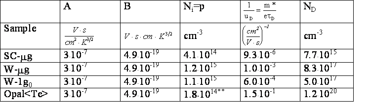
Crystal structure of tellurium


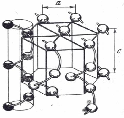
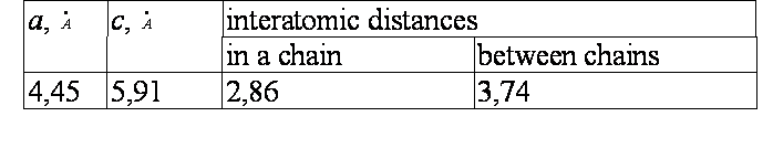
Parameters of tellurium crystal structure

Подпись: Eg=0.33 eV 
Подпись: DE=2.3 meV 
Подпись: 2D1=100 meV 
Подпись: 2D2=126 meV
Подпись: Conduction band 
Подпись: Valence band 
Подпись: D2=63 meV 
Подпись: kz 
Подпись: Brillouin zone of tellurium and isoenergetic surfaces of holes.


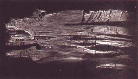
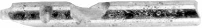
        Tellurium crystal solidified in microgravity SC-mg


                                                    X-ray image of the surface obtained upon cleavage of sample grown by partial remelting of the monocrystal. The arrow shows the starting point of crystallization. Hole concentration p ~ Ni and Nel.active.D for the SC-mg sample.

    X - mobility for the Czhochralski Te crystal.


Подпись: Octahedral cavity 
Подпись: Tetrahedral cavity 
Подпись: Octahedral cavity
Подпись: Tetrahedral cavity
Подпись: Opal structure 
Подпись: Electron microscope image of tellurium cluster lattice in opal 
Подпись:  
Подпись: 500 nm


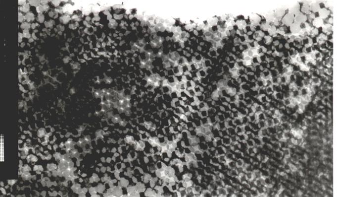
Tellurium cluster lattice in opal with a replica of the octa- and tetrahedral voids as viewed with an electron microscope. Opal crystal filled by Te from a melt under high gas pressure P~3 kBar. Regularly distributed black spots a cluster lattice in the opal matrix (white spots - amorphous silica SiO2 spheres with diameter d~200 ¸ 250 nm).

Electron microscopy image of an opal silica sphere

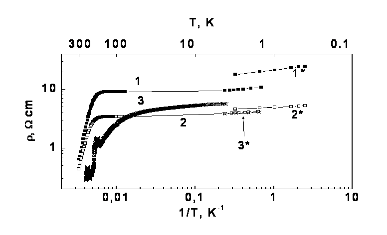
Temperature dependencies of electrical resistivity r for W-mg (1), W-1g0 (2) and Opal<Te> (3) samples. 1*, 2* the data of measurements in the helium temperature range using platinum contacts fused into a sample. 3* - the repeated measurements.

1) r (mg)>r (1g0) and r(Opal<Te>) in the low temperature range.
2) High temperature parts of the curves correspond to the transition to the intrinsic conductivity (Energy gap in Te Eg(0)=0.334 eV).
3) The resistivity at helium temperatures is determined by the electrically active and neutral impurities and grain boundaries.
The resulting inverse mobility for the SC-mg sample can be represented by the Matthiessen's rule:
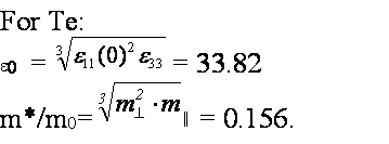

The temperature dependencies of the mobility are attributed to three factors:
–  scattering on phonons predominated at temperatures higher than 30K(1/uL ~ T-3/2).
–  scattering on charge centers prevailed at low temperatures (1/ui ~ T-3/2/Ni).
–  scattering on the defects which limits the maximum value of the hole mobility (1/uD~ND, supposedly independent of temperature).

The values of parameters in Eq. 1 for  various Te samples.

** - determined from Tinv of RH.

Temperature dependencies of the Hall coefficient for the monocrystalline SC-mg sample and W-mg microstructure sample, remelted at microgravity conditions, compared with the parameters for W-1g0 opal<Te> samples, made at the earth conditions. (R at 300 K has the negative sign).

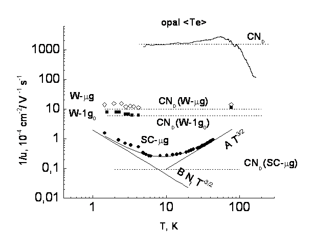
Temperature dependencies of the reversal hole mobility for the monocrystalline SC-mg sample and W-mg microstructure sample, remelted at microgravity conditions, compared with the parameters of the W-1g0 and opal<Te> samples, made at the earth conditions. Points are for the experimental data, curves are for calculation using the Eq.1 with parameters, showed in Table 1. Straight lines - contributions of  scattering mechanisms for the SC-mg sample. Dashed lines – main contributions of the CND term  to the minima of 1/u value.

Determination of the defect concentration ND.

Modulation of the mobility at 77 K and defect concentration ND along the W-mg and W-1g samples, calculated using above equations. For comparison the electrical resistivity profile, r300K(q) along the W-mg sample is shown.


The behavior of the magnetoresistance for the single crystal SC-mg , microstructure samples W- Te and Opal<Te> samples at low temperatures.

Conclusions

• For the first time we have studied the temperature and magnetic field behavior of the electrical resistivity and MR for two kinds of a block structure of Te: the microcrystalline structure in ingots grown during rapid spontaneous solidification under microgravity conditions and the nanocluster Opal structure formed after filling of the opal voids by melted Te.
• In the case of complete melting and re-solidification of Te in mg without a seed, the initial undercooling of the melt followed by spontaneous nucleation and solidification resulted in a raicrocrystalline structure with oscillating the neutral-defect concentration and crystalline orientation along the ingot. The maxima of the resistivity r300K as well as ND profile correspond to the region of ingot surface contacts with the walls ordinary appeared under mg conditions.
• The sensitivity of the electrical properties of Te at low temperatures to the distribution of both neutral and electrically active defects allowed to determine the impurity and defect profiles along the ingot length at the level of 10-5%, which could not be achieved by other methods.
• The rough decrease of the hole mobility (in one order) and the positive AMR in low magnetic fields for the W-mg ingot indicate the predominant hole scattering on neutral defects and boundaries (ND~1018 cm-3).
• In the opal samples we have got the regular structure of contiguous clusters of Te with 2D conducting faces. The physical properties of such 2D conducting ordered system (low mobility, weak localization effect, anisotropy) are determined by both the interface effects between the Te nano clusters and the SiO2 amorphous spheres and the symmetry of the Te sublattice. The positive AMR of this conducting system at low temperatures is a result of the interface scattering of 2D-holes in contrast to a bulk Te crystal where AMR is always negative.

The last update was made on November 25, 2004
Web-Master