see also Si. Mobility and Hall Effect
and Si. Mobility and Hall Effect
 (1396-4315x) cm2 V-1
s-1
 x
x  0.3,
300 K
  (450-865x) cm2 V-1
s-1
 x
x  0.3,
300 K
| Si1-xGex see also Si. Mobility and Hall Effect and Si. Mobility and Hall Effect |
Remarks | Referens | |
| Mobility electrons μn |  (1396-4315x) cm2 V-1
s-1 (1396-4315x) cm2 V-1
s-1 |
0  x x  0.3,
300 K 0.3,
300 K |
Schaffler F. et al.(2001) |
| Mobility holes μp |  (450-865x) cm2 V-1
s-1 (450-865x) cm2 V-1
s-1 |
0  x x  0.3,
300 K 0.3,
300 K |
The mobility is influenceed by alloy scatttering witch contributes according
to μalloy ~ T0.8/(x-x2) (single crystals).
Near band crossover (x 0.15) intervalley
scattering has to be taken into account.
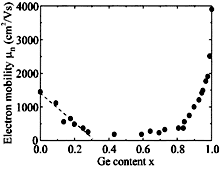 |
Si1-xGex. Electron Hall mobility vs.composition
at 300 K Landoldt-Bornstein (1982, 1987), Sasaki et al. (1984). |
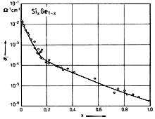 |
SixGe1-x. Intrinsic conductivity
vs.composition. T=300 K Busch & Vogt. (1960) |
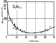 |
SixGe1-x. Electron Hall mobility
vs.composition. T=300 K open symbols -- Busch & Vogt. (1960); Polycrystalline samples were employed in the range 0.3 < x < 0.8. |
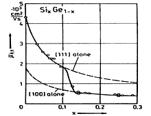 |
SixGe1-x. Electron Hall mobility
vs.composition. x < 0.3. Dashed curves -- calculated mobilities for electrons in [100]- and [111]-valleys. Solid curve -- both types of valleys into account and includes an arbitrary form of intervalley scattering Glicksman (1958) |
 |
Si1-xGex. Electron Hall mobility vs.composition.
T=300 K open symbols -- Busch & Vogt. (1960); full symbols -- Landoldt-Bornstein (1982, 1987) Polycrystalline samples were employed in the range 0.3 < x < 0.8. |
 |
SixGe1-x. Hole Hall mobility vs.composition.
T=300 K Busch & Vogt. (1960) |
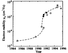 |
Si1-xGex. Evolution of the published
low-temperature electron Hall mobilities. Two-dimensional electron gas in modulation-doped strained Si quantum wells on relaxed Si1-xsGexs barriers (xs  30%). 30%).Schaffler(1997) |
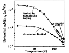 |
Si1-xGex. Electron Hall mobility
vs. temperature of strained Si quantum wells on relaxed Si0.7Ge0.3 For lower curve the mobility is limited by threading dislocations originating from the Si1-xGex buffer layer. Upper curve -- background doping limits the mobility. Sheet carrier densities for both curves are 7 x 1011 cm-2. Corrected room temperature mobility of the two-dimensional carriers is 2500 cm2 V-1 s-1 Schaffler (1997). |
 |
Si1-xGex. Hall mobility vs. measured
carrier density. T= 300 K For comparison, the 300 K mobility of undoped bulk Si is marked Nelson et al. (1993). |
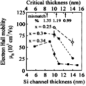 |
Si1-xGex. Electron Hall mobility
vs. Si channel thickness for modulation-doped Si/Si0.7Ge0.3
heterostructures. T= 20 K The mobility drop beyond a channel of 100 A is caused by misfit dislocation formation in the channel. Ismail et al. (1994). |
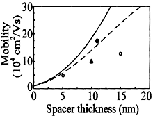 |
Si1-xGex. Calculated electron
mobilities vs. thickness of the undoped spacer layer between the doping
layer and the quantum well. T= 1.5 K, ΔEc = 180 meV, Nd = 2 x 1018 cm-3 Dashed lines -- acceptor background doping levels of 1014 cm-3 Solid lines -- acceptor background doping levels of 1015 cm-3 Stern & Laux (1992). |
 |
Si1-xGex. Calculated carrier
concentrations vs. thickness of the undoped spacer layer between the
doping layer and the quantum well. T= 1.5 K, ΔEc = 180 meV, Nd = 2 x 1018 cm-3 Dashed lines -- acceptor background doping levels of 1014 cm-3 Solid lines -- acceptor background doping levels of 1015 cm-3 Stern & Laux (1992). |
Two-dimensional hole gases can be realized in pseudomorphic Si1-xGex
layers on a Si substrate. The experimental mobilities, however, remain far behind
theoretical predictions.
An alternative route is the realization of pure Ge channels on a relaxed Si1-xGex
buffer with 0.6 < x < 0.8, or of Ge-rich Si1-xGex
channels (x < 0.7) on relaxed Si1-xGex
buffers with 0.3 < x < 0.5. Room temperature mobilities of around
1000 cm2 V-1 s-1 where reported by Arafa
et al. (1996) for such a configuration with a Si0.3Ge0.7
channel.
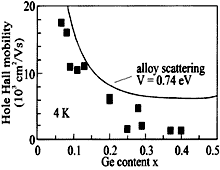 |
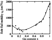
Si1-xGex. Low-temperature hole
Hall mobilities vs. Ge content in pseudomorphic Si1-xGex
quantum wells on Si substrates Data points -- Whall (1995) Solid line -- calculated curve for alloy scattering only, using a scattering potential of 0.74 eV Schaffler(1997) |
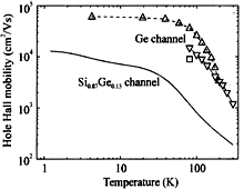 |
Si1-xGex. Hole Hall mobility vs.
temperature in strained Ge channel on cubic Si0.3Ge0.7
buffer and in pseudomorphic Si0.87Ge0.13 quantum well
Schaffler(1997) |