Groups staff:
- Prof. Victor M. Ustinov - leader
- Prof. Vladimir G. Dubrovskii
- Dr. Anton Yu. Egorov
- Prof. Alexei E. Zhukov
- Dr. Alexei R. Kovsh
- Dr. Nikolai A. Maleev
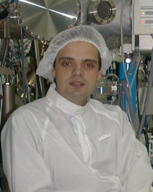
- Dr. Vladimir V. Mamutin photo
- Dr. Daniil A. Livshits
- Dr. Sergei S. Mikhrin photo
- Mr. Alexander Kuzmenkov photo
- Ph.D. student Alexei P. Vasil'ev photo
- Ph.D. student Elizaveta S. Semenova photo
- Ph.D. student Ekaterina V. Nikitina
- student Vladimir V. Odnobludov photo
- Mr. Alexei B. Erin - technician photo
- Mr. V. V. Kislinskii - technician photo
|
|

list of papers |
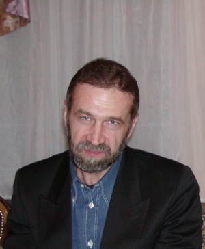
Vladimir Dubrovskii
Was born October 15, 1965, Leningrad, Russia
Education
1982 - 1988 - Leningrad State University, Physical faculty
1991 - 1992 - Oxford University, Department of Engineering Science, Post-doctoral research fellowship sponsored by the RACAL group
Dissertations:
- 1990 - PhD Physics of devices, technique of physical experiments, automation of physical research ("Kinetic models for the kinetics of clustering and thin film growth")
- 2002 - Doctor of Science Condensed matter physics ("Kinetic models of formation of space-ordered structures on solid surfaces")
Work experience:
- 1988 - 1989 – Institute for Analytical Instrumentation RAS (IAI RAS), laboratory of mass-spectrometry, St.-Petersburg. Research engineer
- 1989 - 1992 - IAI RAS, laboratory of mass-spectrometry. Junior research scientist
- 1992 - 1995 – IAI RAS, laboratory of epitaxial nanotechnologies. Senior research scientist
- 1995 - 1998 - IAI RAS. Executive secretary
- 1998 – 2002 - Scientific Instruments PLC, St.-Petersburg. Research director
- from 2002 - Ioffe Physical Technical Institute RAS, laboratory of physics of semiconductor heterostructures. Leading research scientist
Research interests:
Kinetic theory of nanostructure formation during MBE, in particular theory of quantum dot formation in the InAs/GaAs and Ge/Si systems
Kinetics of thin film growth on solid surfaces
Theory of ordering effects on solid surfaces
Kinetic theory of nanowhisker formation
Theory of first order phase transitions, nucleation and condensation
Adsorption and desorption, adsorbate dynamics
MBE technologies of A3B5 growth
List of publications includes more than 100 papers.
mail to |
|
|

list of papers |
Alexey E. Zhukov
Alexey E. Zhukov was born in 1968 in St. Petersburg (former Leningrad), Russia.
He received the M.S. degree in physics from the Leningrad Electrical Engineering institute in 1992 and the Ph.D. degree in physics from the Ioffe institute in 1996.
Since 1992 he has been working at the A.F.Ioffe Physico-Technical institute, Russian Academy of Sciences (St.Petersburg, Russia) currently as a senior researcher. His research is concentrated on molecular beam epitaxial growth of III-V quantum-sized hetetrostructures. He has a particular interest in design, growth and study of self-organized quantum dot structures for laser and VCSEL applications. He and his collaborators have published over 200 articles in journals and conference proceedings.
26 December 2002 Alexey Zhukov was awarded with Doctor of Physical-Mathematical Sciences(short thesis (rus) .pdf file)
mail to |
|
|
|
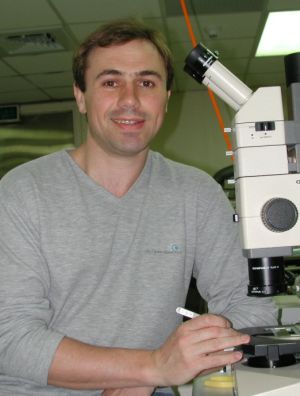
Alexey R. Kovsh
Alexey Kovsh was born in 1973 in St-Petersburg, Russia.
He received the M.S. with honors (1996) in Optoelectronics from the St-Petersburg Electrical Engineering University and Ph.D. (1999) in Semiconductor Physics from Ioffe Institute.
His research interests are MBE growth of semiconductor heterostructures based on (In, Ga, Al,)(As, N) material system, study the effect of structure design and growth condition on optical, structural and electrical properties of high electron mobility transistors, short-period superlattices, and device performance of edge-emitting and vertical cavity surface emitting lasers (VCSELs) based on quantum wells and quantum dots.
From 1996 to 1999, he was a Ph.D. student in Ioffe Institute and since 1999 he has been working as a researcher of the same institution. During this time he spent all together more than two years working as a visitor scientist in Heinrich-Hertz Institute, Berlin (1999), and in Industrial Technology Research Institute, Taiwan (2000-2002) within joint scientific programs with Ioffe Institute.
He has authored over 100 papers in refereed journals and conference proceedings.
mail to |
|
|

list of papers |
Nikolai A. Maleev
Was born March, 1, 1966, Leningrad, USSR
Education
1989 - Leningrad Electrical Engineering Institute (currently Electrical Engineering University of St. Petersburg), Chair – Dielectrics and Semiconductors (with honors)
Career and research experience
“Svetlana-Electrondevices Co.”, St. Petersburg
- 1989-1992 – engineer
- 1992 -1995 - senior engineer
- 1995-1998 – senior engineer, head of research group
A.F.Ioffe Physico-Technical Institute, Russian Academy of Sciences, Laboratory of Physics of Semiconductor Heterostructures
- 1998-present time – research scientist
1997 - Candidate of Technical Sciences (Electrical Engineering University of St. Petersburg) PhD thesis: “Capacitance-voltage methods for analysis of GaAs Schottky barrier microstructure”
Area of expertise:
Physics and design of microwave semiconductor devices (microwave GaAs Schottky diodes, MESFETs, HEMTs, HBTs, varactor diodes), numerical modeling, MBE-growth and fabrication of vertical-cavity surface-emitting lasers, capacitance-voltage profiling of multi-layer structures
Number of papers in refereed journals and conference proceedings: >60
mail to |
|
|
|
Daniil A. Livshits
Daniil A. Livshits was born in 1968 in St. Petersburg, Russia.
He received the M.S. degree in physics in 1993 from the St. Petersburg State Technical University and the Ph.D. degree in physics in 2000 from the Ioffe institute.Since 1990 he was working at the A.F.Ioffe Physico-Technical institute, Russian Academy of Sciences (St.Petersburg, Russia) currently as a researcher-scientist. His research is concentrated on edge-emitting laser diodes and VCSELs based on novel design and new materials A(III)B(V)-system.
Developed projects:
- Al-free high power lasers (l=0.76-0.86mm)
- Study of facet degradation processes of high power lasers
- Semiconductor power amplifiers (SOA)
- Spontaneously formed periodical InGaAsP structures and laser with this active region
Managed projects:
- High power single mode InGaAs/GaAs lasers
- High power InGaAsN 1.3mm lasers
Skills
- Edge emitting and VCSEL design,
- design and deposition of optical coatings for lasers and SOA
- reactive ion etching RIE
- developing metal deposition for omic contacts
- chipping and bonding, devise packaging
- Device and structures characterization (photoluminescence, electrical, short pulse, optical, cryotemperature measurements)
- Developing hardware of dielectric coating deposition system, die-bonding, measurement setups
He has co-authored over 100 papers in refereed journals and conference proceedings
mail to |
|
|

|
Ekaterina V. Nikitina
was born in St. Petersburg (at that time Leningrad), Russia in 1977.
Education
- 1990-1994 - Physical-mathematical school (a department of St. Petersburg State Electrotechnical University) graduated with honors
- 1994-2000 - of St. Petersburg State Electrotechnical University, A.F.Ioffe Physico-Technical Institute (Department of Electronics) graduated (a master diploma)
- 2000- present time - Ph.D. study in St. Petersburg State Electrotechnical University, A.F.Ioffe Physico-Technical Institute
Job career
- 1997-2001 - Probationer in Ioffe Physical-Technical Institute (out of staff) during education.
- 2001-present time - Probationer-researcher in Ioffe Physical-Technical Institute.
|
|

|