SiGe | Remarks | Referens | ||
Energy gaps, Egindirect (Δ conduction band min) | Si1-xGex | 1.12-0.41x + 0.008x2 eV | 300 K, x < 0.85 | |
Si (x=0) | 1.12 eV | 300 K, x = 0. | see Si. Band structure | |
Energy gaps, Egindirect
(L conduction band min) | Si1-xGex | 1.86 - 1.2x eV | 300 K, x > 0.85 | |
Ge (x=1) | 0.66 eV | 300 K, x = 1. | see Ge. Band structure | |
| ||||
Conduction band | ||||
Energy separation EΓ1 | Si1-xGex | 4175 - (2814 ± 55)x meV | 70 K; 0 < x < 0.3, Linear Fitting Si1-xGex films on Si substrates | Ebner et al. (1998) |
Si (x=0) | 3.4 eV | 300 K | see Si. Band structure | |
Ge (x=1) | 0.8 eV | 300 K | see Ge. Band structure | |
Eg(Γ-X) | Si1-xGex | 0.8941 + 0.0421x+ 0.1691x2 | calculated | Krishnamurti et al. (1983) |
Eg(Γ-L) | Si1-xGex | 0.7596 + 1.0860x+ 0.3306x2 | calculated | Krishnamurti et al. (1983) |
Energy separation EΓ2 | Si1-xGex | (3400 ± 7) - (300 ± 40)x meV | 70 K; 0 < x < 0.3, Linear Fitting Si1-xGex films on Si substrates | Ebner et al. (1998) |
Si (x=0) | 4.2 eV | 300 K | see Si. Band structure | |
Ge (x=1) | 3.2 eV | 300 K | see Ge. Band structure | |
| ||||
Valence band | ||||
Energy of spin-orbital splitting Eso | Si1-xGex | 0.044 + 0.246x eV | 300 K | |
Si (x=0) | 0.044 eV | 300 K, x = 0. | see Si. Band structure | |
Ge (x=1) | 0.29 eV | 300 K, x = 1. | see Ge. Band structure | |
Effective conduction band density of states | Si1-xGex | ~ 2.8 x 1019cm-3 | 300 K, x < 0.85 | |
Si1-xGex | ~ 1.0 x 1019cm-3 | 300 K, x > 0.85 | ||
Si (x=0) | 2.8 x 1019cm-3 | 300 K, x = 0. | see Si. Band structure | |
Ge (x=1) | 1.0 x 1019cm-3 | 300 K, x = 1. | see Ge. Band structure | |
Effective valence band density of states | Si (x=0) | 1.8 x 1019cm-3 | 300 K, x = 0. | see Si. Band structure |
| Ge (x=1) | 0.5 x 1019cm-3 | 300 K, x = 1. | see Ge. Band structure |
| ||||
Intrinsic carrier concentration | Si1-xGex | see Si1-xGex. Intrinsic carrier concentration | ||
Si (x=0) | 1 x 1010 cm-3 | 300 K, x = 0. | see Si. Band structure | |
Ge (x=1) | 2 x 1013 cm-3 | 300 K, x = 1. | see Ge. Band structure | |
Energy Gaps vs. Composition | ||||
E1 | Si1-xGex | 3452 - (1345 ± 25)x meV | 70 K; 0 < x < 0.3, Linear Fitting Si1-xGex films on Si substrates | Ebner et al. (1998) |
E'1 | Si1-xGex | 5402 ± 25 + (280 ± 120)x meV | ||
E2 (X) | Si1-xGex | 4351 ± 38 + (210 ± 180)x meV | ||
E2 (Σ) | Si1-xGex | 4518 ± 129 + (880 ± 600)x meV | ||
Eg(Γ-X) | Si1-xGex | 0.8941 + 0.0421x+ 0.1691x2 | calculated | Krishnamurti et al. (1983) |
Eg(Γ-L) | Si1-xGex | 0.7596 + 1.0860x+ 0.3306x2 | calculated | Krishnamurti et al. (1983) |
![]() | Band
structure of Si at 300 K.
| ||||||||||||||||||||
![]() | Band
structures of Ge.
|
![]() | SixGe1-x.
Indirect Energy gap vs. composition at 296 K One-phonone model of the absorption edge. At about x=0.15 a crossover occurs of the Ge-like [111] conduction band minima and the Si-like [100] conduction band minima Braunstein et al. (1958) |
![]() | Si1-xGex.
Fundamental (indirect) band gap & excitonic band gap at 4.2 K Squares - band gap of Si1-xGex at 4.2 K (absorption measurements) ; Dots - excitonic band gap of Si1-xGex at 4.2 K (photoluminescence measurements) Braunstein et al. (1958) and Weber & Alonso (1989) |
![]() | Si1-xGex.
Composition dependences of several important direct transitions observed. Kline et al. (1968) and Pickering et al. (1993) |
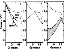
![]() | Si1-xGex
alloys.Fundamental indirect band gap vs. x of pseudomorphic Si1-xGex
(001) alloys: (a) on Si substrate; (b) on Si0.5Ge0.5 substrate; (c) on Ge substrate. Dashed lines - unstrained bulk band gap. Experimental points are taken from Lang et al. (1985) and Dutartre et al. (1991). Solid lines - calculated curves. People (1985, 1986) and Van de Walle & Martin (1986). |
0 < x < 0.3 | Remarks | Referens | ||
EΓ1 | = 4175 - (2814 ± 55)x | meV | 70
K; Si1-xGex films on Si substrates | Ebner et al. (1998) |
EΓ2 | = (3400 ± 7) - (300 ± 40)x | meV | ||
E1 | = 3452 - (1345 ± 25)x | meV | ||
E'1 | = 5402 ± 25 + (280 ± 120)x | meV | ||
E2 (X) | = 4351 ± 38 + (210 ± 180)x; | meV | ||
E2 (Σ) | = 4518 ± 129 + (880 ± 600)x | meV |
Si1-xGex | Compositional dependence of band gaps | Remarks | Referens | |
Eg(Γ-X) | = 0.8941 + 0.0421x+ 0.1691x2 | calculated | Krishnamurti et al. (1983) | |
Eg(Γ-L) | = 0.7596 + 1.0860x+ 0.3306x2 |
x=0 (Si) | Eg = 1.17 -4.73 x 10⁻⁴ x T2/(T + 636) | (eV) | see also Si. Band structure and carrier concentration |
x=1 (Ge) | Eg = 0.742- 4.8x 10⁻⁴·T2/(T+235) | (eV) | see also Ge. Band structure and carrier concentration |
x=0 (Si) | EΓ2 = 4.34 - 3.91·10-4·T2/(T+125) | (eV) | see also Si. Band structure and carrier concentration |
x=1 (Ge) | EΓ1 = 0.89 - 5.82·10-4·T2/(T+296) | (eV) | see also Ge. Band structure and carrier concentration |
![]() | Si1-xGex
alloys. Fundamental indirect band gaps vs. temperature at different
x. Braunstein et al.(1958) |
![]() |
Si1-xGex alloys. Intrinsic carrier concentration vs.
temperature at different x. |
Nc
4.82 x 10¹⁵ · M ·
(mc/m0)3/2·T3/2
(cm-3)
4.82 x 10¹⁵ (mcd/m0)3/2
· T3/2
5.3 ·
1015 x T3/2 (cm-3) ,
where M=6
is the number of equivalent valleys in the conduction band.
mc = 0.32m0 is the effective mass of the density
of states in one valley of conduction band.
mcd
= 1.06m0 is the effective mass of density of states.
Nc 4.82 x 10¹⁵
· M · (mc/m0)3/2·T3/2
(cm-3)
4.82 x 10¹⁵ (mcd/m0)3/2
· T3/2
2 ·
1015 x T3/2 (cm-3) ,
where M
= 4 is the number of equivalent valleys in the conduction band.
mc = 0.22m0 is the effective mass of the density
of states in one valley of conduction band.
mcd
= 0.55m0 is the effective mass of density of states.
x=0 (Si) | Nc![]() ![]() mv = 0.81m0 is the hole effective mass of the density of states. | see also Si. Band structure and carrier concentration |
x=1 (Ge) | Nc![]() ![]() mv = 0.34m0 is the hole effective mass of the density of states. | see also Ge. Band structure and carrier concentration |
x=0 (Si) | Eg=Eg(0)-1.4·10-3P | (eV) | see also Si. Band structure and carrier concentration |
x=1 (Ge) | Eg = Eg(0) + 5.1·10-3P | (eV) | see also Ge. Band structure and carrier concentration |
(&Teta;d + 1/3&Teta;u
- a) (for A valley) | (&Teta;d
+ 1/3&Teta;u - a) (for L valley) | b | &Teta;u | &Teta;u | Remarks | Referens | |
Si | 1.72 eV | -3.12 eV | -2.35 eV | 9.16 eV | 16.14 eV | Theory | Van de Walle & Martin (1986) |
1.5 ±0.3 eV | -2.10 ±0.1 eV | -4.85 ±0.15 eV | Experiment | Laude
et al. (1971), Chandrasekar & Pollak (1977), Balslev (1966) | |||
Ge | 1.31 eV | -2.78 eV | -2.55 eV | 9.42 eV | 15.13 eV | Theory | Van de Walle & Martin (1986) |
-2.0 ± 0.5 eV | -2.86 ±0.15 eV | 16.2 ± 0.4 eV | Experiment | Laude et al. (1971), Chandrasekar & Pollak (1977), Balslev (1966) |
Both the valence and conduction band degeneracy are lifted by the uniaxial [001] strain component, which leads to the following splittings (Van de Walle and Martin, (1986)):
For higher Ge contents, the conduction band becomes Ge-like with electrons being located at the L minimum. With the uniaxial strain component being directed along [001], no splitting of the L minimum occurs for reasons of symmetry.
![]() | Si1-xGex.
Schematic diagram of the relevant band edges of Si subjected to hydrostatic
and uniaxial strain as described in equations. Energy values apply to a tensely strained Si quantum well on an Si1-xGex substrate with x = 30% Schaffler(1997) |
![]() | Si1-xGex.
Contour plots of the conduction ΔEc and valence ΔEv
band offsets of pseudomorphic Si1-xGex layers on cubic Si1-xsGexs
substrates over the complete range of x and xs. The signs correspond to an electronic energy scale, where the active layer (x) is referred to the cubic substrate of composition xs. Exciton-corrected experimental results indicate that for x > xs and x < 0.8, the conduction band offset is 0<ΔEc<+40 meV [Penn et al. (1999)]; that is, for most of the (x,xs) combinations the band alignment is staggered (Type II) with the valence band offset being always in favor of the material with the higher Ge content. The theoretically predicted Type I region for x and xs being larger than about 80% has not been confirmed experimentally Schaffler(1997) |
![]() | Si1-xGex.
Solid lines - Variation of the relevant band edges of a strained Si layer on a cubic Si1-xsGexs substrate . The dashed lines correspond to the substrate bands. LH, light holes; HH, heavy holes; SO, spin-orbit split holes Schaffler(1997) |
![]() | Si1-xGex.
Solid lines - Variation of the relevant band edges of a strained Ge
layer on a cubic Si1-xsGexs substrate . The dashed lines correspond to the substrate bands. . LH, light holes; HH, heavy holes; SO, spin-orbit split holes Schaffler(1997) |
At x < 0.85, Si1-xGex alloys are considered as "Si-like" material: | Remarks | Referens | |
Effective electron mass (longitudinal)ml | 0.92mo | Schaffler F.(2001) | |
Effective electron mass (transverse)mt | 0.19mo | Schaffler F.(2001) | |
Effective mass of density of states
mcd=M2/3 mc (for all valleys of conduction band) | 1.06mo | Son
et al. (1994); Son et al. (1995) | |
Effective mass of the density of states mc=(ml+mt2)1/3 (in one valley of conduction band) | ![]() | ||
Effective mass of conductivity mcc= 3/(1/ml+2/mt) | ![]() |
At 0.85< x <1, Si1-xGex alloys are considered as "Si-like" material: | Remarks | Referens | |
Effective
electron mass (longitudinal)ml | 0.159mo | Schaffler F.(2001) | |
Effective electron mass (transverse)mt | 0.08mo | Schaffler F.(2001) | |
Effective mass of density of states
mcd=M2/3 mc (for all valleys of conduction band) | 1.55mo | Son
et al. (1994); Son et al. (1995) | |
Effective mass of the density of states mc=(ml+mt2)1/3 (in one valley of conduction band) | 0.22mo | ||
Effective mass of conductivity mcc= 3/(1/ml+2/mt) | ![]() |
![]() | Si1-xGex.
Variation of the conduction band effective masses vs. composition Rieger and Vogl (1993) |
Remarks | Referens | |||
Effective hole masses (heavy) mhh | Si (x=0) | 0.537 mo | 4.2 K | see also Si. Effective Masses |
Ge (x=1) | 0.33 mo | see also Ge. Effective Masses | ||
Effective hole masses (light) mlh | Si (x=0) | 0.153 mo | see also Si. Effective Masses | |
Ge (x=1) | 0.0430 mo | see also Ge. Effective Masses | ||
Effective hole masses (spin-orbit-split ) mso | Si1-xGex | (0.23-0.135x) mo | 300 K | Schaffler F.(2001) |
Si (x=0) | 0.234 mo | see also Si. Effective Masses | ||
Ge (x=1) | 0.095(7) mo | 30 K | see also Ge. Effective Masses |
![]() | Si1-xGex.
Valence band dispersion along [100] and [110] for Si0.5Ge0.5
on Si(001). (schematic view) Schaffler F.(2001) |
![]() | Si1-xGex.
Valence band parameters A, B, and |C| vs. composition x Schaffler F.(1997) |
![]() | Si1-xGex.
Heavy hole effective mass density of states mhd vs. energy at different
x . Manku & Nathan (1991) |
![]() | Si1-xGex.
Light hole effective mass density of states mhl vs. energy at different
x . Manku & Nathan (1991) |
![]() | Si1-xGex.
Experimental heavy hole cyclotron masses in strained Si1-xGex
quantum wells. Dots - Cheng et al. (1994), squares - Wong et al. (1995). Dashed line corresponds to unstrained bulk, Bottom solid line is a prediction for strained Si1-xGex |