
1, 1´ n=3·1015 cm-3;
2, 2´ n=4·1016 cm-3;
3 n=2.3·1017 cm-3.
For curve 3 electron and drift mobility values are practically equal.
Symbols are experimental data from several different papers.
Chattopadhyay et al. (1981)

|
Electron drift (dashed curves) and Hall (solid curves) mobility vs.
composition parameter x. T=300 K. 1, 1´ n=3·1015 cm-3; 2, 2´ n=4·1016 cm-3; 3 n=2.3·1017 cm-3. For curve 3 electron and drift mobility values are practically equal. Symbols are experimental data from several different papers. Chattopadhyay et al. (1981) |
 |
Electron Hall mobility versus temperature for Ga0.47In0.53As. 300K Electron concentration no=3.5·1014 cm-3 at 300K. Oliver, Jr. et al. (1981) |
 |
Electron Hall mobility in Ga0.47In0.53As at 77 K for different compensation ratios:
θ=(Nd + Na )/n. 1 - θ=1, 2 - θ=2, 3 - θ=5, 4 - θ=10. Symbols represent the experimental data from several works Pearsall (1982) |
 |
Electron Hall mobility in Ga0.47In0.53As at 300 K for different compensation ratios:
θ=(Nd + Na )/n. 1 - θ=1, 2 - θ=2, 3 - θ=5, 4 - θ=10. Symbols represent the experimental data from several works Pearsall (1982) |
 |
Hall factor for n-type Ga0.47In0.53As (y=1) versus temperature. 1 - no=1015 cm-3, 2 - no=1017 cm-3. Pearsall (1982) |
| µp≤500 | InAs; x=0 | µp≤500 |
| µp≤300 | Ga0.47In0.53As; x=0.47 | µp≤300 |
| µp≤400 | GaAs; x=1 | µp≤400 |
 |
Hole Hall mobility versus temperature for n-type Ga0.47In0.53As. Hole concentration po=5.5·1015 cm-3 at T=300 K. Novak et al. (1989) |
 |
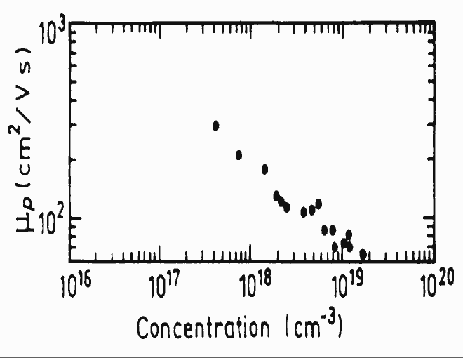
Hole Hall mobility in Ga0.47In0.53As at t=77 K versus total impurity concentration Nd + Na. Pearsall and Hirtz (1981) |
 |
Hole Hall mobility in Ga0.47In0.53As at t=295 K versus total impurity concentration Nd + Na. Pearsall and Hirtz (1981) |
 |
Temperature dependence of the electron mobility µn (1) and sheet electron density n2DEG (2) in
Ga0.47In0.53As/Al0.48In0.52As heterostructure. Doping density in AlInAs layer is equal to 3·1017 cm-3. T=300 K. Matsuoka et al. (1990) |
 |
Hall electron mobilities of pseudomorphic GaxIn1-xAs/Al0.48In0.52As
MODFET versus indium content at two temperature. 1 - 77 K 2 - 300 K Pamulapati et al. (1990) |
| µn cm2/Vs | 2DEG density, cm-2 | |||
| x | 300 K | 77 K | 300 K | 77 K |
| 0.25 | 14100 | 113000 | 1.71·1012 | 1.65·1012 |
| 0.20 | 15200 | 123100 | 1.84·1012 | 1.81·1012 |
| 0.15 | 15300 | 70700 | 1.84·1012 | 1.81·1012 |
 |
Electron mobility versus 2D carrier density at 300K for pseudomorphic HEMT structures AlGaAs/GaxIn1-xAs/(Al)GaAs. H- homogeneously doped structures, P- planar doped structures. For H1-15, H2-15, P-15 and 2P-15 samples x = 0.15. For P-25 and 2P-25 x=0.25 Gaonach et al. (1990) |
| n2DEG (1012 cm-2) | µn (cm2/V·s) | |||
| 300 K | 77 K | 300 K | 77 K | |
| Sample A | 4.3 | 2.5 | 3910 | 18400 |
| Sample B | 8.8 | 6.0 | 2710 | 6540 |
| Sample C | 6.2 | 4.1 | 4630 | 19100 |
| Sample D | 2.0 | 1.8 | 5600 | 22000 |
 |
Hole Hall mobility (1) and 2DHG density (2) versus temperature for single strained GaAs/Ga0.8In0.2As/GaAs quantum well structure. Fritz et al. (1986) |
 |
Hole Hall mobility at 76 K versus 2D carrier density for 90 A -thick GaAs/Ga0.8In0.2As/GaAs single strained quantum well. Fritz et al. (1986) |
|
|